

In our modern world of wireless mobile connectivity, print can be viewed as a uniquely analog and peculiarly offline media; as compared to digital, print is distinctly unconnected, static and isolated. As a form of visual communications, print is the penultimate monomedia. It is dependent upon typography and its linear consumption, i.e. left to right (in the West), top to bottom. Print is the antithesis of hypermedia.
Look at your bookshelf; each book is a veritable communications island “entire of itself.” Even with tables of contents and indices (indexes), our printed books are hyperlink deprived; and, though they sit next to and touch each other, they cannot “connect.”
Taking a longer view, ink-on-paper media is the legacy of industrial era communications technology in the digital age. In the future, as Benny Landa explained at DRUPA2012, mankind will no longer communicate by “smearing pigment onto crushed trees.”
What’s that? This is a very one-sided viewpoint. What about the unique properties of paper and print that no digital and mobile media can replicate? What about the dimensional and tactile elements of the print media experience? What about the environmental benefits of paper-based products? Yes, these are valid arguments against the supremacy of digital over analog media.
Alongside these great features of print, there is another aspect that is either misunderstood or unknown. Conventionally speaking, print is not a form of electronics; but, in a very profound sense, electronics is actually a form of print. From the earliest days of the electronics revolution, printing methods were used to design and manufacture transistors, integrated circuits and microprocessors. From the beginning of the digital age, photolithography and photoengraving techniques were used to make semiconductors.
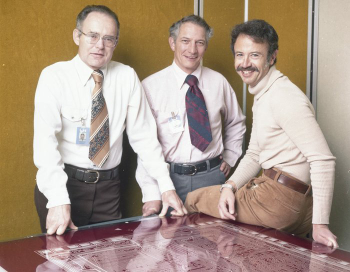
In fact, the pioneers of electronic devices—including Robert Noyce and his team of physicists and chemists at Fairchild Semiconductor, who invented the microchip, and later at Intel, who invented the microprocessor—used the same techniques that printers used to prepare plates for press. Light tables, ruby masks, cameras and film were the standard tools of the electronics industry in Silicon Valley throughout the 1950s, 60s and 70s. And photolithography methods still remain critical steps in sectors of the electronics industry to this day.
While many of the most modern and sophisticated electronics components such as CPUs have moved beyond their photoengraving roots—mainly due to limitations of scale—the relationship between these technologies has continued to evolve. Over the past decade, printed electronics (PE) has become a new and promising merger of these two seemingly opposed disciplines.
PE is the production of electronic components—displays, memory, batteries and sensors—by applying layers of conductive and nonconductive inks onto plastic, cloth or paper. PE uses many of the same methods that are familiar in commercial printing: screen printing, flexography, gravure, offset lithography and inkjet.
Although it is still in the early stages of development, PE is being driven by the promise of significant cost savings. Electronics manufacturing requires precision placement of layers of conductive material in intricate patterns. With previous photoengraving methods, which are subtractive, multiple steps are required to create each layer and much of the material is etched away and unused during the process. With PE, an additive process, each layer is created in as few as two steps—printing and curing—and all of the applied conductive material gets used.

One practical example of PE is printed radio frequency identification (RFID) tags. RFID is a wireless system that uses radio-frequency fields to transfer data from a tag on an object to a reading device for automatic identification and tracking. RFID tags made with conventional silicon manufacturing methods can cost as much as $25 each. These devices are being currently used widely in the logistics and retail industries at the container level.
The expectation is that PE will bring the cost of RFID tags down to one cent or a fraction of one cent. Once this is accomplished, nearly every object produced can have its 2D barcode replaced with an RFID tag. Imagine being able to go to the market, load up your shopping cart and—without stopping at the checkout—have your account billed for your purchases and wheel that buggy right out to your car. What a time saver!
There are many other applications of PE in research and development. The advancements in conductive ink technologies, along with the microscopic precision in their application to substrates with PE, raises the possibility that every object in the world can be made into a “smart” object that is capable of interactivity and data collection.

The proliferation of smart sensors such as RFID tags and other wireless electronic devices is connecting objects to one another and to the Internet in the tens of billions. Kevin Ashton, the technology pioneer who came up with the phrase “The Internet of Things,” wrote the following about this phenomenon in 2009, “We need to empower computers with their own means of gathering information, so they can see, hear and smell the world for themselves, in all its random glory. RFID and sensor technology enable computers to observe, identify and understand the world—without the limitations of human-entered data. … The Internet of Things has the potential to change the world, just as the Internet did. Maybe even more so.”
So, in our brave new world of wirelessly connected objects, printed electronics has a very important role to play, especially in package and label production. As it turns out, print is actually becoming a most electronic and connected media. Perhaps, with the application of printed electronics to replace ISBN barcodes and the Dewey Decimal System labels, even the books in our analog libraries will be able to interact with each other after all.
